

The next AI supply-chain trade may not be another GPU, HBM stack or CoWoS capacity line. It may be the material underneath the package. As AI accelerators become larger, denser and more power-hungry, the substrate that connects chips, memory and power delivery is becoming part of the performance limit.
Investors often simplify the issue as "PCB limits," but the more precise bottleneck is the advanced package stack: organic package substrates, interposers and the routing layer that lets GPUs, HBM and chiplets talk to each other. Traditional materials are not disappearing. They are mature, cheap and still good enough for most electronics. The question is whether the largest AI and HPC packages need a new foundation.
Why Traditional Substrates Are Hitting A Wall
AI chips are changing the rules of packaging. The trend is not just one larger GPU. The package now needs to place GPUs, HBM, chiplets and high-speed I/O closer together. More pieces inside one package mean more connections, tighter routing, greater power delivery stress and a larger physical footprint.
Organic substrates still have a long future, but ultra-large AI packages make their weaknesses more visible. Larger substrates can warp. Higher-speed signals can lose more energy. Denser routing becomes harder. Yield and cost become more fragile as the package area expands. For a phone or a normal PC, those limits may not matter much. For a next-generation AI accelerator, they can become the difference between a workable package and a bottleneck.
TrendForce reported that as substrate sizes expand, warpage becomes one of the major hurdles for mass production in panel-level packaging. That is why glass is being discussed not as a fashion material, but as a possible answer to a physical scaling problem.
The Industry Is Still In Qualification Mode
The most important point for investors is timing. Glass substrates are not yet a broad revenue story. They are a qualification story. Pilot lines, samples, customer validation and yield learning matter more than headline excitement.
TrendForce's glass-substrate overview says TSMC unveiled a 310×310 mm CoPoS product line in 2025, plans to establish a first mini production line at VisEra in 2026, begin small-volume trial production in 2027 and reach mass production between 2028 and 2029. The same report says Samsung established its first mini production line through Samsung Electro-Mechanics for glass core substrates in 2025, with mass production scheduled for 2027.
That timeline is why the trade is early. A company can be real, technically important and still several years away from meaningful sales. The market may price the possibility before the income statement shows it, but the gap between qualification and revenue is where most of the risk lives.
Why Glass Could Become A Mainstream AI Packaging Material
Glass does not need to replace every organic substrate to become a major theme. It only needs to become important in the highest-value part of the market: AI accelerators, HPC packages, advanced chiplets and high-bandwidth memory integration.
The reason is simple. AI chips are increasingly constrained by how efficiently the package can connect, power and cool the silicon inside it. LPKF describes glass interposers and glass core substrates as two paths for high-density advanced packaging, arguing that glass can address warpage, dielectric loss and dimensional instability as AI and HPC architectures scale. Corning's semiconductor glass materials similarly highlight low electrical loss, high stiffness and through-glass via opportunities.
The mainstream path is likely selective. Glass can first appear where customers care more about performance, density and power efficiency than about the lowest possible substrate cost. If yield improves and costs fall, the addressable market can widen. If yield remains difficult, glass may stay in premium AI/HPC designs rather than becoming a broad electronics standard.
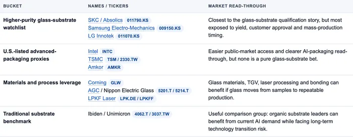
A Short Watchlist
What Could Make The Trade Work?
The bullish path needs evidence. Customer qualification is the first major catalyst. A clear link to Nvidia, AMD, Broadcom, Apple, Amazon, TSMC or Samsung would matter because the technology needs design-in credibility, not just laboratory proof.
Pilot-line progress is another catalyst. Headlines about samples can move sentiment, but pilot-to-mass-production conversion is what turns a theme into revenue. Investors should also watch through-glass via yield, micro-cracking, RDL precision, warpage control and panel-level processing cost. Those details may sound technical, but they decide whether glass remains an expensive showcase technology or becomes a scalable packaging platform.
AI package size is the demand-side trigger. If next-generation accelerators keep adding HBM, chiplets and larger package formats, glass becomes more relevant. If organic substrates, silicon interposers or other advanced-packaging approaches solve the same problems cheaply enough, glass adoption could move more slowly.
What Are The Risks?
Promising does not mean proven. Glass can crack, warp or suffer via-related defects if the process is not controlled at scale, and the cost curve still matters. If glass remains too expensive, adoption may stay concentrated in the most expensive AI and HPC packages rather than becoming a broad packaging standard.
Timing is another risk. Many roadmaps point to 2027–2029, which means 2026 may still be more about qualification, sampling and customer validation than revenue. Alternative technologies are also improving: organic substrates, silicon interposers, CoWoS, fan-out and hybrid approaches can all slow glass adoption if they solve enough of the same problems at lower cost.
The investment risk is that the theme moves faster than the orders. Small, high-purity names can rally on glass-substrate headlines before mass-production yield or customer volume is proven. U.S.-listed names such as INTC, TSM, AMKR and GLW are easier to access, but none is a pure glass-substrate bet. For higher purity, the watchlist moves toward Korea, Japan and specialty equipment names such as SKC/Absolics, Samsung Electro-Mechanics, LG Innotek, AGC, Nippon Electric Glass and LPKF.
Glass substrates are not a guaranteed overnight replacement for traditional substrates. The stronger thesis is that AI chips are getting too large and too complex for today's packaging stack to scale easily, and glass offers one of the clearest paths to larger, denser and more energy-efficient packages. The winners will be the companies that can prove customer qualification, manufacturable yield and real exposure to next-generation AI packaging.